
Samsung pushes boundaries with its next-generation flagship processor as Exynos 2700 “Ulysses” chip leaks surface on Geekbench. Early benchmark listings reveal an experimental deca-core SoC built on a cutting-edge 2nm process, signaling the company’s aggressive plans for superior efficiency and performance in future Galaxy devices. Spotted on an Engineering Reference Device running Android 16, this chip highlights Samsung’s focus on advanced power management and AI-ready capabilities.
While the Galaxy S26 series prepares to launch with the Exynos 2600, these Exynos 2700 “Ulysses” chip leaks offer an exciting glimpse into 2027’s potential powerhouse. Industry insiders note that Samsung deliberately uses mixed-generation cores in testingiphenyl to optimize Android’s energy-aware scheduling, setting the stage for smarter, more efficient smartphones.
Exynos 2700 “Ulysses” Chip: Revolutionary Deca-Core CPU Architecture
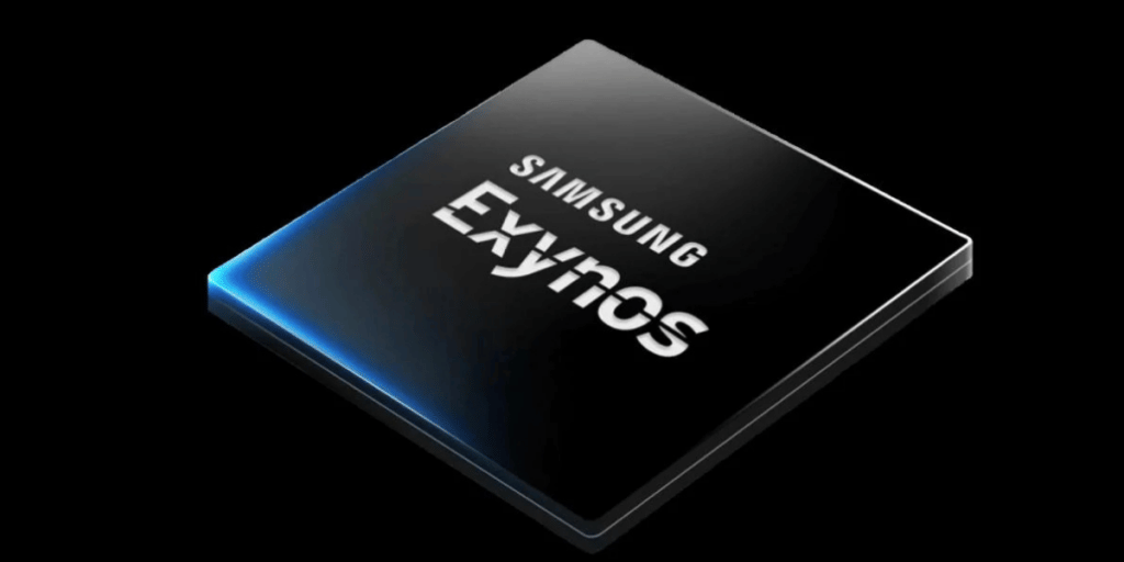
The Exynos 2700 “Ulysses” adopts an unconventional “4+1+4+1” cluster setup, marking a departure from traditional designs:
- 10 cores total: Features four distinct speed tiers for optimized task handling.
- Clock speeds: 1x core at 2.30GHz, 4x cores at 2 2.40GHz, 1x core at 2.78GHz, and 4x cores at 2.88GHz.
- Testing focus: Samsung mixes core types to refine software scheduling and power efficiency under Android 16.
Benchmark scores remain modest at this early stage, as engineers prioritize stability over raw performance.
Advanced GPU, Memory Support, And 2nm Process
Samsung equips the Exynos 2700 “Ulysses” with forward-thinking components to handle demanding AI and graphics workloads:
- Xclipse 970 GPU: Delivers an initial OpenCL score of 15,618, with significant improvements expected through driver and thermal optimizations.
- Next-gen memory and storage: Supports upcoming LPDDR6 RAM and UFS 5.0 for faster data handling in AI applications.
- SF2P 2nm node: Utilizes second-generation Gate-All-Around transistors for better power efficiency and performance.
These Exynos 2700 “Ulysses” chip leaks underscore Samsung’s shift toward in-house manufacturing excellence. By proving its foundry capabilities, the company aims to reduce reliance on external partners like TSMC. Consumers won’t see this chip in devices until 2027, but the promising early data builds anticipation for Samsung’s 2nm-era dominance in the smartphone space.
Are you still browsing through your broken screen? Don’t worry! Book at-home mobile phone screen repair with Cashify—an affordable and one-stop destination for all your mobile phone needs. In case you break your screen within 1 month of repair, we will replace your screen again—for FREE.